This Blog is part of a Series! Check out the rest if you haven’t already:
- Home Security & I’m Back: A story about how I built my own security system and wrote some software for it.
- Alarm System Part 1: The Old Security System: What came with the house when I bought it, and an overview of the chips on the board and a deep dive into how the EEPROM works.
- Alarm System Part 2: System Teardown: Tearing out the EEPROM and socketing it for testing.
- Alarm System Part 3: Dumping the EEPROM
- Alarm System Part 4: The Keypad: What’s making this thing work?
- Alarm System Part 5: How to Hack a Home Security System: Getting in!
I’ve recently built my own home security panel. For the code, STLs, and a rambling blog about it, look over here.
What does a technology hoarder do with the old system components you probably didn’t ask?
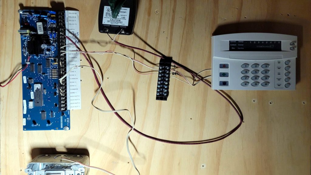
I took the existing components and strapped them to a board. It’s cool, because you can see the entirety of the system (sans siren) in one spot. Makes it easier to understand if you haven’t worked with these systems before.
Sadly, since I don’t have the siren in place, the board detects that it is missing and panics for service. Whatever, I’ll drag out a ladder and complete it eventually. But for now, I wanted to understand what the board is doing.
I’ll preface this by saying I’m not an alarm installer, an electrical engineer, and a lot of the stuff I’m doing in these blogs are first times for me. I’m going to chronicle the story as it happened with all of the failures intact, not to build trust, but because screwing up is fun. I haven’t wrote or dumped an EEPROM before, eavesdropped on a SPI bus, modified or attempted to dump existing chip ROMs. But I think I’ll start.
For obvious reasons, I can’t share all that I find because, while I welcome a lawsuit, I prefer those I can win.
First step was to take a picture of the board and figure out what the ICs are for:
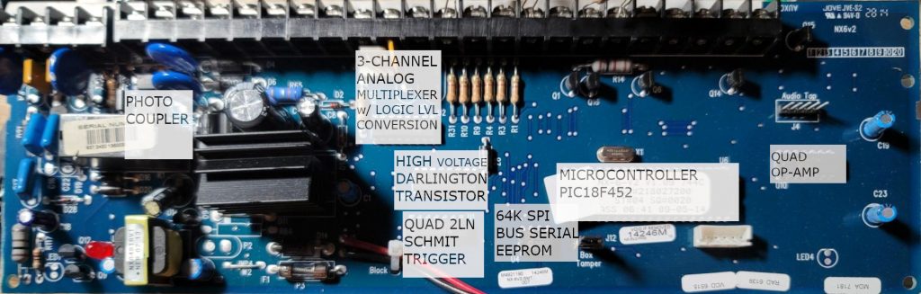
We know that the code can be set, and updated, so we have to store the PIN the panel uses somewhere within these chips. I’m not convinced the microcontroller has the ability to persist information after powerloss (but I’ll need to read the datasheet to know for sure).
The one I’m mostly interested in is the wordy “64K BUS SERIAL EEPROM” which I know because I threw the IC number into DuckDuckGo and got a sexy datasheet back. Knowing this can be read and wrote on the fly, and persist during power loss means this is the most likely place for the PIN to be stored. The lame part is that the EEPROM’s capacity is 8,192 bytes — and I’ll be looking for a specific four. I’m hoping, for that reason, that most of the information on this EEPROM is just NUL’d out, but I have no idea yet.
I have two options to answer my question:
- Wait a few weeks until Father’s Day. My wife is getting me the Ben Eater 6502 breadboard computer and an EEPROM programmer. I can simply just wait until that shows and dump the contents (I might, not sure yet)
- I can, still pretending I know everything Ben Eater knows, read the datasheet and get an idea of how I’ll need to interact with it.
For the folks who have read (or performed) ROM dumping on older cartridges, you’ll know those are just EEPROM chips — but they’re often parallel — so you’ll have a series of A# lines and D# lines — address and data, which convince the EEPROM to spit out the data stored on them.
If this device has 8,192 data addresses, we’d need 14 individual lines at a minimum to access the data, and for each byte to be output, we’d need another 8. Then, you’d want something for Vdd, Vss, a clock, and a way to trigger read/write. So our chip would need 26ish pins. At least this makes perfect sense in my head. I could be wrong, pay attention in future blogs if I admit this.
The chip in front of us, however, is a bit different.
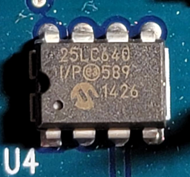
This chip has 8 pins, so to access all that data, we’re going to have to break out some cereal.

Serial*
So, we’ll go dive into the datasheet I linked above and see what we can figure out.
First we need to figure out what voltage we’re at. I’m going to assume based on what other chips are here.
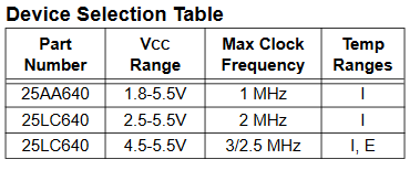
Our part number is one of the two lower parts, so we’re looking at one really tolerant of typical 3.3v logic levels and 5v. And one that is clearly just cool with 5, but is EXTREMELY FASTTTTTT.
The microcontroller this panel uses is a PIC18F452-IP, which has a girthy 332-page datasheet that I won’t be reading. Thankfully, they had this microcontroller under a sticker to keep prying eyes from somehow peeling it off.
Annoyingly, the datasheet didn’t help at all, specifying a wide range it operates at, and that there is a special “Low Voltage Detection” module that can trigger cleanup tasks before powerdown.

So, I walk away still unsure exactly what this is. So, time to reference the board again.
I notice a fat heatsink on here that reeks of voltage regulator — or amplifer. Assuming it may be an amp for the siren, I’m going to keep looking around.
There’s also a logic level converter on the board which tells me it’s probably using multiple. I suspect even if the board natively runs at 3.3v, I can still interact with the chip at 5v if it’s tolerant, since both are.
As a final attempt to identify this, let’s look over at the crystal to read the obvious and clear frequency off of that:
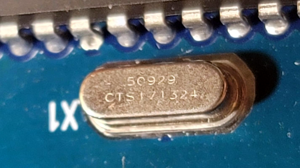
Of course not, so I found a site where I can upload a picture of my crystal and it’ll identify it. It didn’t work.
Jokes aside, I found out it’s a 20MHz oscillator, so that won’t help be identify it either. It was close to the microcontroller, so the microcontroller must be handling the timing for the EEPROM at a frequency it likes.
I did notice a few “Warranty void if removed” stickers, and thankfully, I wasn’t removing any stickers.
Benching the EEPROM
Whether I decide to wait for the programmer or throw it on a breadboard, I’ll have to understand the chip either way, so we’ll run through the process of breadboarding it.
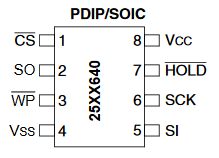
First, we have to understand the pinout:
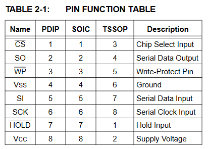
We’re only planning on reading it, so the write protect pin will come in helpful. We can also only focus on reading operations (I think, not sure if I can ignore serial write when I have to send a command to read bytes — find that out later).
First, we’d hook up Vcc to +5vDC and Vss to -5vDC, the rest I have zero idea right now.
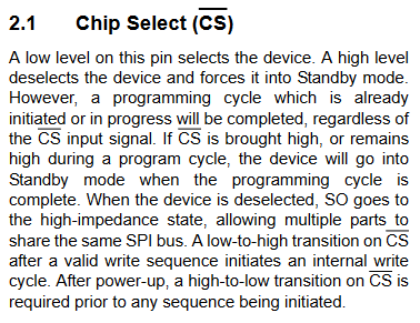
Hey, documentation! We do have the option of interfacing with multiple different chips if we want to. It’s like in class when the teacher calls on you, she pulls you low and… wait. No, you pull the CS pin low (ground) and it tells the chip we’re talking to it. There’s only one chip we’re breadboarding, so we’ll just tie this low (to ground).
This serial output will be the chip’s mouth — this is where we’ll need to set up an input that reads on the falling edge (transition from high to low state) of the serial clock.
Again, we’re not looking to overwrite the EEPROM, so we can just tie this to low.
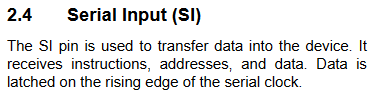
Damn it, looks like I will need to pay attention to SI as well, since we need to send instructions to get data back.
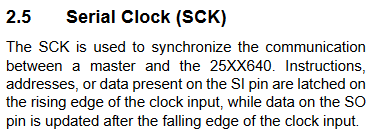
The clock is how we maintain a heartbeat with the EEPROM, to indicate state changes. This will be tied to an output pin on the Arduino.
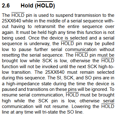
I’m under the impression that this will just need to be tied high for my use case.
Let’s Have a Conversation!
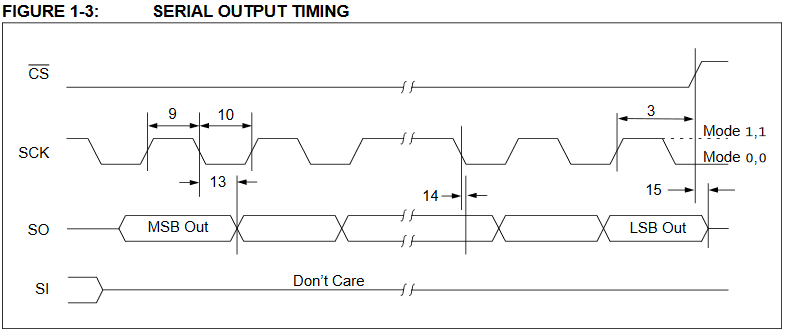
This timing diagram will help us digest the data streaming from the EEPROM. Based on what I’m seeing here, the SO (Serial Out) will maintain a bit value for an entire clock cycle. You’ll see the MSB (most significant bit) is sent during the entire rising edge, high state, and falling edge of the SCK (Serial Clock). So, we can send a high value to the clock, read the value, drop the clock and repeat. Also good to note from this is MSB comes before LSB — so we’re looking at big endian output.

It’s midnight. We’ll dig into more timing diagrams and instruction routines in the next blog!
Leave a Reply